


- Customer: Fu Chang Electronic Technology Co., Ltd.
- Industry: Electronics
- Country: China
- Solution: Moldex3D eDesign
- View PDF Version
Executive Summary
In order to reduce costs and energy consumption, CAE technology for injection molding has been widely applied in various industries. Fu Chang also utilizes this technology in producing cell phone cases, telecommunication, and other products. In this case, through Moldex3D eDesign simulation solution, Fu Chang was able to predict the plastic filling behavior and potential problems that might occur during the injection molding process. With the valuable simulation analyses, Fu Chang could directly address the problematic issues by further optimizing the gating design, the cooling channel layout and other molding conditions prior to the actual production in order to achieve the most optimal results. Thus, Fu Chang’s goal to reduce materials and the cycle time could be achieved while, at the same time, improving the final product quality.
Challenges
- Warpage
- Weld line
- Stress marks
Solutions
Fu Chang used Moldex3D eDesign to validate product design (Fig 1) and mold design in the early development process. According to Moldex3D analysis results, gating and geometry designs were changed for product design optimization and the design changes were further tested and analyzed through simulation technology.
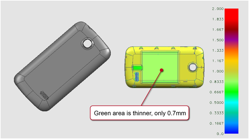 Fig. 1 Product design
Case Study
The main purpose of this project was to find out the most optimized gating design, cooling channel layout and molding parameters in order to solve the molding problems such as filling difficulties, excessive pressure and warpage due to the thin, lightweight product design through Moldex3D simulation solution. Currently, using 3-gate or multi-gate design is quite common in today’s practice when manufacturing mobile/cell phone products. However, using this kind of gating design can cause uneven pressure distribution and lead to product shrinkage and warpage (as shown in Fig. 2). As a result, the product will require post-processing work to conceal the defects and the production cost will increase. This kind of design is prone to weld line formation, which can only be concealed by a heavy coating of spray. However, in order to obtain the finest product quality with aesthetic attributes that maximize the appeal to customers, this method is no longer applicable. It will also lengthen product cycle time.
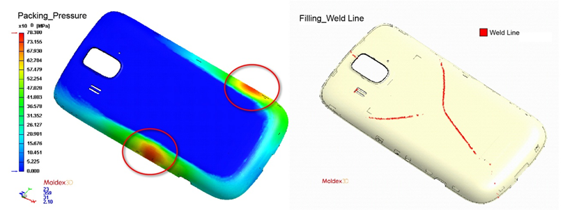 Fig. 2 Conventional 3-gate design causes uneven pressure distribution (as the red circles show on the left)
and visible weld lines (as the red lines show on the right)
To solve this problem, Fu Chang used Moldex3D eDesign to find out the most suitable gate design, changing the original 3-gate design to a 1-gate design (Fig 3). According to the analysis results, this gating design change greatly improved the pressure distribution and successfully solved the warpage issue caused by uneven shrinkage. In addition, the occurrence of weld line formation could be significantly minimized to having only minor, naturally formed weld lines around the hole region due to the original geometry design and these minor defects could be concealed entirely by increasing the mold temperature in the later stage in the injection molding process.
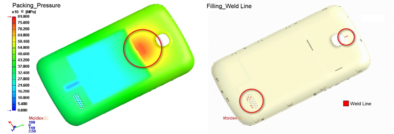 Fig. 3 Changing to a 1-gate design, the pressure near the gate is higher (as shown in the red circle on the left), but the pressure distribution in other areas is more even. Also, the occurrence of weld line formation could be significantly minimized to having only minor defects (as shown in the red circles on the right).
In addition to the gating design issue, the original product design also encountered stress marks induced by uneven thickness geometry design. Therefore, using the 1-gate gating design, Fu Chang added a transition zone in the area where the thickness changes (Fig 4).
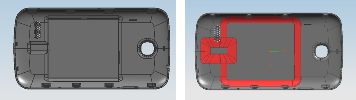 Fig. 4 The central part in the original product design is thinner (left). A transition zone is added in the area where the thickness changes in the optimized design (right).
After the design changes, Fu Chang used Moldex3D eDesign to simulate both the original design and the optimized design. The analysis results of the original product design showed (Fig5) an obvious shear stress concentration in the area where the thickness changes will occur, resulting in the formation of visible stress marks. In the optimized design, there is no obvious shear stress concentration area; the surface defects can be eliminated successfully and the final product will have a smooth surface. Furthermore, when comparing with the actual mold trial results, Fu Chang found that Moldex3D simulation analysis results were strongly correlated with the results from the actual mold trial (Fig 6).
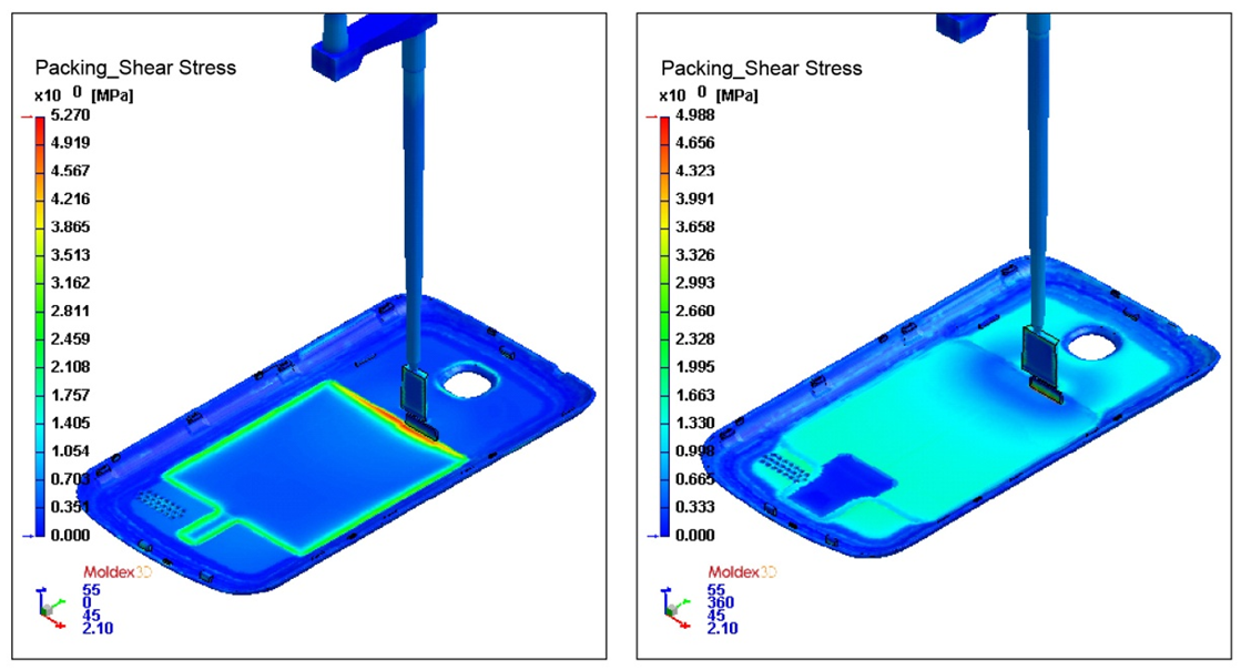 Fig 5 . The simulation analysis results show the original design has obvious shear stress concentration due to the uneven thickness (left), and the optimized design does not have obvious shear stress concentration (right).
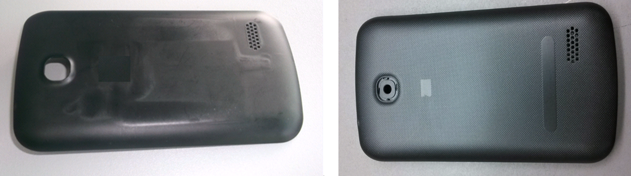 Fig. 6 The actual mold trial results showed the original design has visible stress marks due to uneven thickness (left), and the optimized design does not have this issue (right). The actual mold trial results were strongly correlated with the simulation results.
In short, Moldex3D eDesign allowed the user to simulate different gating design changes, cooling channel layouts, and material and molding parameter changes including filling time, filling pressure, screw locations, cooling temperatures and molding cycle. Through Moldex3D eDesign, Fu Chang was able to analyze the original design comprehensively, find out the potential problematic areas, address the issues on weld lines, warpage, and pressure distribution directly, and ultimately achieve the most optimal results to reduce the cycle time and improve product quality.
Benefits
The final results showed that the pressure was reduced by 20% and the warpage displacement was successfully controlled within the acceptable range. More specifically, the warpage displacement in the X-axis direction was improved by 50%; 55% in the Y-axis direction, and 30% in the Z-axis direction (Fig 7). The typical manufacturing difficulties when producing thin, lightweight products, such as weld lines, surface defects, and unbalanced pressure distribution, could be well-addressed and overcome. These improvements shortened the cycle time, and further reduced the production cost by eliminating the unwanted expense spent on the post-processing tasks.
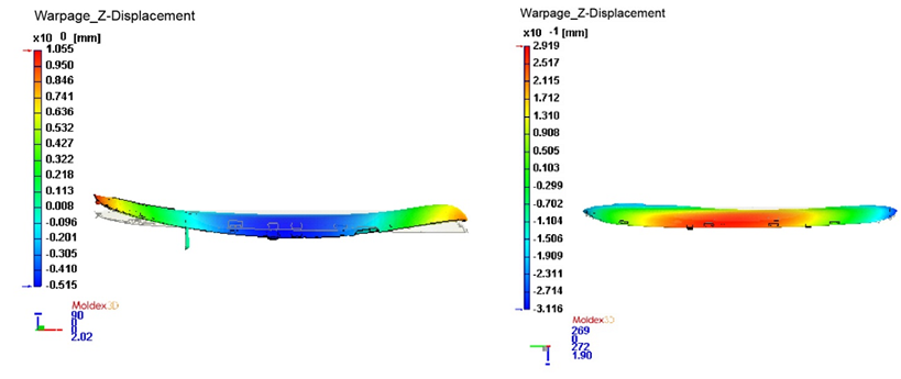 Fig. 7 The warpage displacement in the Z-axis direction of the original design (left)
and the significant improvement on the warpage displacement of the optimized design (right)
Through the aid of Moldex3D eDesign solution, Fu Chang was able to get prompt simulation analyses for multiple design changes to find out the most feasible and optimal product design and manufacturing parameters before the actual production. The potential product defects could also be predicted by the simulation software and prevented in advance. Thus, the product quality was greatly improved and the overall production cost was significantly reduced. Once again, Moldex3D has proven to be a reliable and smart tool for product optimization and design validation.