
EDA tools that perform physical layout-IC, IC package, or PCB- are generally two dimensional and may work fine for substrate layout, interconnect planning, or metal fill creation. Toward the design complexity and density involved for today’s IC packages, three dimensional design and simulation are driven to more realistically design, manage, and verify the multi-tier wire bond die or stacked-die designs.
The Cadence® Connections™ EDA Program works with third-party software suppliers around the world to enhance the value that customers find in using Cadence products. The program supports and embraces suppliers that offer complementary solutions in front-end design, verification IP, IC implementation, mixed-signal, verification, manufacturability, and system-package-board. The Cadence EDA tool meets the need by providing IC package designers with the capability to physically visualize a design as it will actually look during manufacturing. A designer can interactively zoom, pan, and rotate the 3D view for their IC package design [1].
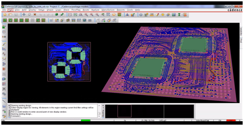 Fig. 1 Cadence EDA tool visualizes the design of IC package
Moldex3D IC Packaging analysis currently enables an interface for users of Cadence EDA tool to further enhance the packaging design-to-manufacturing process through the innovative and professional 3D simulation technologies. This interface between Cadence and Moldex3D enables you to import the .3di file in Moldex3D Designer and Mesh for your complex IC packages design. Once all the components have been seamlessly imported in Moldex3D pre-processor, an automatic and efficient mesh generator allows meshing of the complete package geometry with minimal model simplification. In addition, a parametric capability facilitates a proper mesh creation for delicate IC wires, thereby greatly saving time and efforts spent on mesh preparation.
Furthermore, Moldex3D can calculate the resin flow considering nonlinearities such as viscosity change of epoxy molding compound during both in-mold and post-mold curing process. Significant molding problems can be predicted and solved upfront, which helps engineers enhance chip quality and prevent potential defects more efficiently [2]
 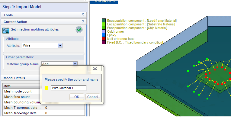 |
Fig. 2 Moldex3D pre-processor provides an interface for 3di file and the parametric capability for delicate IC wires
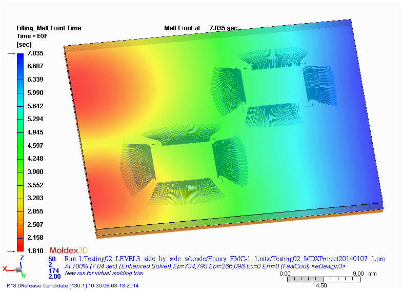 Fig. 3 Moldex3D IC packaging visualize 3D simulation and predict potential molding defects
[1] https://www.cadence.com/products/pkg/3d_design_viewer/pages/default.aspx[2] https://www.youtube.com/watch?v=nj3ltW7Ax1c