- Date:Jun 02, 2026
- Location: San Jose, CA, USA
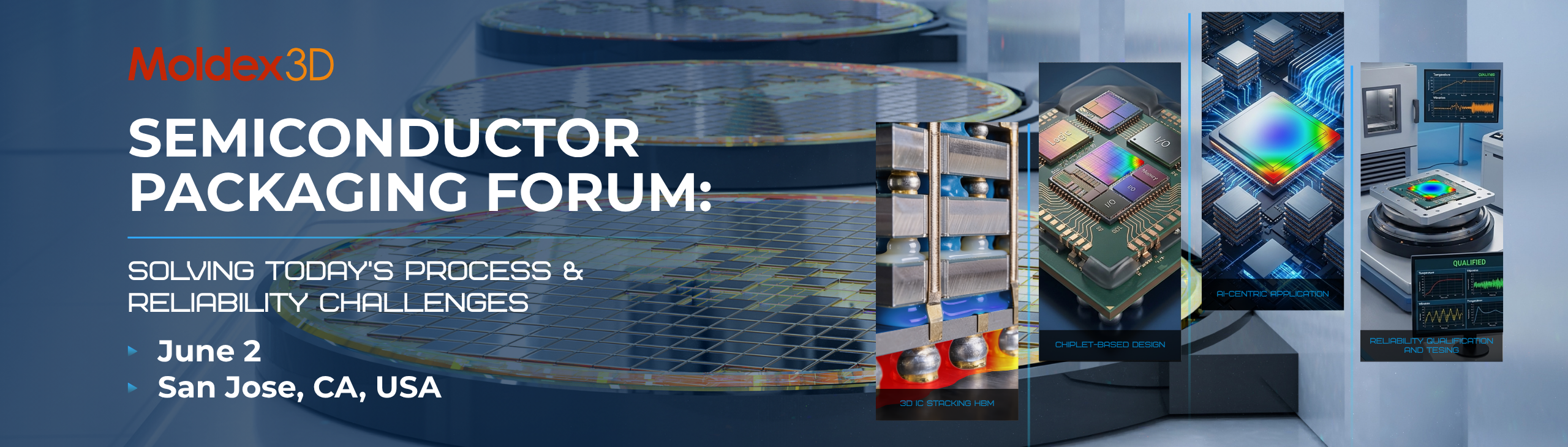
Solve what breaks in semiconductor packaging—before it reaches production
Join a focused, small-group forum on eliminating voids, controlling fillet and overflow, and reducing warpage through simulation-driven insight.
Semiconductor packaging teams are under increasing pressure to deliver smaller, faster, and more reliable devices—across both traditional transfer molding and advanced processes such as underfill, potting, and encapsulation—driven in part by emerging architectures like HBM, chiplet-based designs, and AI-focused applications. Yet critical issues such as void formation in underfill and encapsulation, fillet control, overflow, wire sweep, and package warpage are often only discovered late in development—leading to costly iterations, qualification delays, and reliability risks.
This half-day, in-person forum brings together industry experts to explore how these challenges can be addressed earlier through simulation-driven approaches. Hosted by Moldex3D, the sessions will highlight how combining process simulation with structural and multiphysics analysis provides deeper visibility into encapsulation behavior, stress development, and long-term package reliability—before tooling and production.
Through real-world case studies and technical discussion, attendees will learn how to:
- Predict and reduce voids, fillet inconsistencies, overflow, and wire sweep in underfill, potting, encapsulation, and transfer molding processes
- Understand and mitigate warpage and residual stress to improve package integrity and yield
- Reduce design iterations and qualification cycles to accelerate development and lower cost
This is a focused, small-group event designed for practical learning and open discussion with peers facing similar challenges.
Agenda
| Time (PT) | Session | Presenter |
| 8:45 AM – 9:00 AM | Arrival/Sign-In | |
| 9:00 AM – 9:05 AM | Welcome & Industry Overview | Moldex3D |
| 9:05 AM – 9:35 AM | Why Packaging Fails—and How to Fix It Using Simulation Case Studies Real-world examples addressing voids, fillet control, overflow, and late-stage failures |
Moldex3D |
| 9:35 AM – 10:05 AM | Transfer Molding for Traditional Packaging Improving process control, reducing variability, and increasing yield before tooling |
Moldex3D |
| 10:05 AM – 10:15 AM | Break | |
| 10:15 AM – 10:45 AM | Mastering Encapsulation in Advanced Packaging—From Underfill to Potting and Dotting Controlling flow behavior, material placement, and process consistency across encapsulation methods |
Moldex3D |
| 10:45 AM – 11:15 AM | Understanding and Controlling Warpage Across the Package Map Predicting deformation and improving package reliability early |
Moldex3D |
| 11:15 AM – 12:00 PM | Q&A | Moldex3D |
Venue
Holiday Inn San Jose Silicon Valley
1350 North First Street, San Jose, CA 95112
Contact
Srikar Vallury
E: sales.us@moldex3d.com
P: 248-946-4570