- Date:Apr 01, 2022
- Location: India
- Time: 11:30 AM IST

Upcoming Dates
| Date | Time | |
| April 1, 2022 | 11:30 AM IST | Closed |
Description
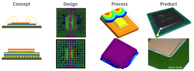
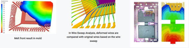
Plastic Chip Encapsulation is a molding process where chips are being capsulated with Epoxy Molding Compound (EMC) to prevent physical damage or corrosion. This process contains the interconnection between microchips and other electronics (so-called wire bonding), curing phenomenon of thermoset material, and various control management of process conditions. Due to the complexity of multiple material components, such as EMC, chip, or lead frame, and high wire density, many challenges and uncertainty have been brought to the Chip Encapsulation process. Common defects include incomplete fill, air traps, voids, wire sweep, paddle shift, package warpage, etc
What You Will Learn
Moldex3D IC Packaging provides a complete series of molding solutions, and supports comprehensive solutions such as: Transfer Molding, Molded Underfill, Capillary Underfill (CUF), Compression Molding, Embedded Wafer Level Package (EMWLP), and No Flow Underfill (NFU) / Non-Conductive Paste (NCP). Auto meshing function supports for user to complete encapsulation analysis more easily. User also can adopt advanced manual meshing for more complex component like undercut-shaped lead frame.
Moldex3D IC Packaging helps designers to fully analyze the chip encapsulation process from filling, curing, cooling, to advanced manufacturing demands, such as filler concentration, underfill encapsulation, post-molding curing, stress distribution, or structural evaluation. Significant molding problems can be predicted and solved upfront, which helps engineers enhance chip quality and prevent potential defects more efficiently. The accurate simulation also helps design optimization and well cost management.
Contact
For sales & technical inquiries, please write to Khaled EL Bchiri at khaled.bchiri@moldex3d.com