- Date:Aug 27, 2020
- Location: Americas
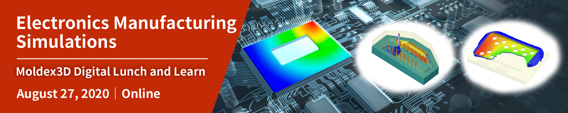
Manufacturing of components used in the electronics industry involves complex processes such as underfill and potting. Challenges faced during such processes often include part quality issues such as voids and warpage. During this session, attendees will learn how to simulate and visualize such potential defects using Moldex3D. A demo on setting up an IC Packaging simulation will also be provided in this session.
Register below and come join us!
Agenda
| Time (PST) | Session | Presenter |
| 11:30 AM – 11:45 AM | Log-in | |
| 11:45 AM – 12:00 PM | Introduction | |
| 12:00 PM – 12:30 PM | Flow Simulation of the Potting Manufacturing Process for an Electronic Device | Moldex3D NA |
| 12:30 PM – 1:00 PM | Simulation of the Capillary Driven Encapsulation Process | Moldex3D NA |
| 1:00 PM – 1:30 PM | Warpage and Void Simulations of System in Package | StatsChipPack/JCET |
| 1:30 PM – 2:15 PM | Moldex3D IC Packaging Demo | Moldex3D NA |
| 2:15 PM – 2:30 PM | Q & A | |
Contact
Justin Guth
T: 248-946-4570 ext. 329
E: justinguth@us.moldex3d.com