According to IC Insights’ 2012 McClean Report, “The assembly and packaging of ICs no longer takes a back seat to front-end processing…packages have evolved from simple cookie-cutter type packages to highly sophisticated and customized solutions.” Perhaps this is mirrored in the latest industry trend that semiconductor manufacturers are eager to enter the packaging arena, and it is expected that with the growing popularity of 3D IC, the capital expenditure on packaging will keep growing in the following years.
Today, semiconductor fabrication plants have invested considerable resources and research on 3D IC process because of the benefits brought by wafer-level packaging technology. Traditional semiconductor device assembly companies also focus on 3D IC process due to a huge global demand for microchips.
3D IC brings many benefits, such as its superior capability to increase chip performance and functionality, lower power consumption, greater storage capacity, more bandwidth, and reduced chip size. However, the process also has to overcome thermal and reliability challenges. For example, epoxy molding compound used to protect the silicon chip, solder bumps, wire bonds, lead frame, and paddle in IC encapsulation technology may also cause structure deformation and induce unwanted defects.
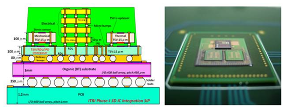
 Fig. 1 Schematic of a 3D IC structure. Image source : ITRI, Electronics and Optoelectronics Research Laboratories.
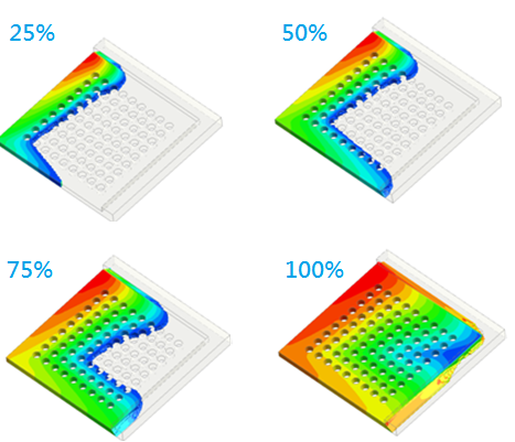
Moldex3D has been developing and delivering solutions to challenges of real-world IC encapsulation process for many years. Moldex3D Encapsulation solution provides accurate predictions on wire sweep, residual stress, void and so on. Due to the growing demand for 3D IC packaging industry, Moldex3D develops the flip chip molding simulation as a powerful tool for investigating 3D IC reliability during packaging stage as shown in figure 2. Process challenges in fine pitch flip chip process, such as mechanical shock and voids for underfill on-site process caused by complex interactions between flowing reactive polymer melt and microchip components, can be easily differentiated from the heat transfer of Moldex3D simulation, structural deformation and curing kinetics of the underfill in microchips.
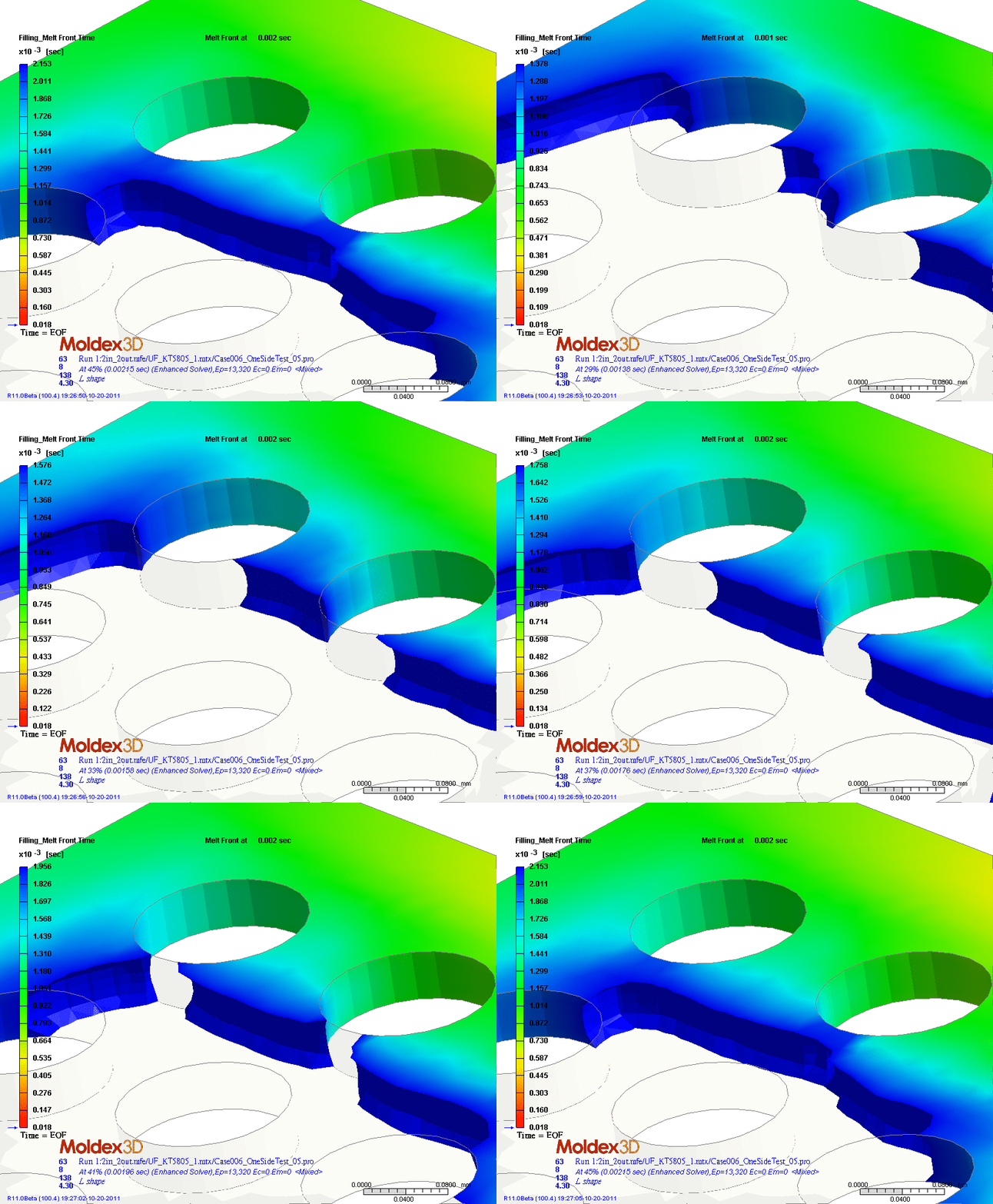
The capillary flow behavior, as illustrated in figure 3, governed by the surface tension of underfill, the contact angle between bumps and substrate, and dispensing process are all considered in numerical analysis. Moldex3D Encapsulation demonstrates how encapsulant fills gap, flows around the bumps, and effects of moving speeds of the injector; no more time will be wasted on understanding those complicated physical phenomena. By utilizing the simulation capability of Moldex3D, process designers can ensure IC package reliability and high performance.
For more information about Moldex3D IC package solution, please proceed to read Tips and Tricks- “How to Set up Wire Sweep Analysis in Moldex3D” or submit your questions or comments here.


Fig. 2 Simulation of capillary underfilling flow front Fig. 3 Simulation of capillary flow behavior